
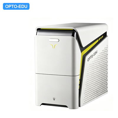
Opto Edu A63.7016 Benchtop Tungsten Filament Scanning Electron Microscope, SE+BSE+EDS, 100000x
-
إبراز
benchtop tungsten filament SEM
,scanning electron microscope with EDS
,100000x magnification electron microscope
-
دقة130 فولت
-
تسارع الجهد5 كيلو فولت، 10 كيلو فولت، 15 كيلو فولت
-
مرحلة العينة المتحركة ثلاثية الأبعادX:±25 مم Y:±25 مم Z:30 مم
-
الحد الأقصى لحجم العينة"90 ملم (قطر) 40 ملم (سمك)"
-
بندقية الكترونخيوط التنغستن خرطوشة مركزة مسبقا
-
إشارة الصورةالإلكترون المرتد
-
مكان المنشأالصين
-
اسم العلامة التجاريةCNOEC, OPTO-EDU
-
إصدار الشهاداتCE, Rohs
-
رقم الموديلA63.7016
-
وثيقة
-
الحد الأدنى لكمية1 جهاز كمبيوتر
-
الأسعارFOB $1~1000, Depend on Order Quantity
-
تفاصيل التغليفالتعبئة الكرتون ، لنقل الصادرات
-
وقت التسليم5 ~ 20 يوما
-
شروط الدفعT/T ، West Union ، PayPal
-
القدرة على العرض5000 جهاز كمبيوتر شخصى / شهر
Opto Edu A63.7016 Benchtop Tungsten Filament Scanning Electron Microscope, SE+BSE+EDS, 100000x
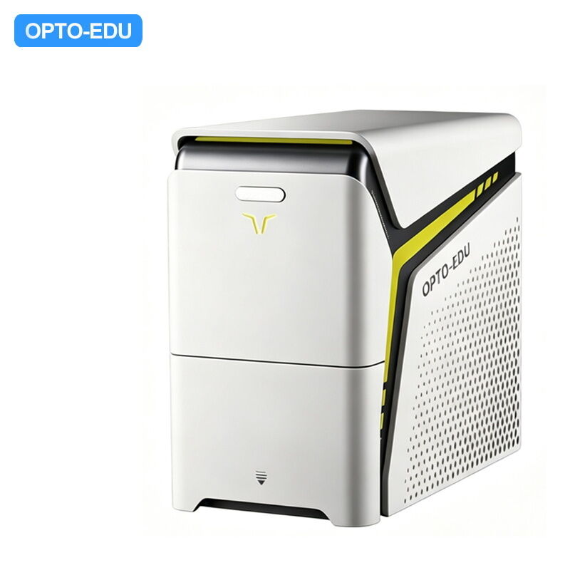
Opto Edu A63.7016 Benchtop Tungsten Filament Scanning Electron Microscope
SE+BSE+EDS, 100000x magnification

Advanced Analytical Performance
The A63.7016 SuperSEM breaks tradition with real-time EDS elemental analysis, combining SEM and EDS technologies in an advanced electron optical system. With exceptional analytical performance, real-time energy-dispersive spectroscopic pseudo-color imaging, and user-friendly operation, it enables in-depth analysis of both surface structure and chemical elements of samples.
A63.7016 SuperSEM Key Features
- Always display X-ray spectra in real-time
- Real-time Energy Dispersive Spectroscopy (EDS) Pseudo-color Imaging
- Highlight elements of interest during analysis
Technology Overview
The scanning electron microscope uses an electron beam as the illumination source, irradiating samples with a focused, fine electron beam in a raster scanning manner. This generates various information related to sample properties, which is collected and processed to obtain magnified images of microscopic morphology. Compared to optical or transmission microscopes, it offers high resolution, large depth of field, and three-dimensional imaging capabilities.
Performance Advantages
- Fast Scanning Speed: Signal acquisition bandwidth up to 10M. Video mode allows real-time sample observation without ghosting or trailing, ensuring no detail is missed.
- Compact Design: Structurally efficient device requires no special equipment rooms or additional vibration isolation tables. Plug-and-play with standard mains power, suitable for limited laboratory space.
- Advanced Coloring Technique: SEM image coloring visually highlights sample details, enhancing feature recognition and facilitating analysis. Color differentiation can reveal material composition, improving research outcomes.
- Real-time Spectral Comparison: Quantitative results display in real-time without completing collection, allowing comparison with previous spectra during the collection process.
- Visualized Energy Spectrum Analysis: Freely select analysis ranges for points, lines, or surfaces. Excellent visualization algorithms achieve precise separation of close spectral peaks and display elemental spatial distribution for studying material characteristics.
Technical Specifications
| Specification | A63.7016 | A63.7016-X | A63.7016-V | A63.7016-L |
|---|---|---|---|---|
| Resolution | 130eV | 130eV | 130eV | 130eV |
| Acceleration voltage | 5 kV, 10 kV, 15 kV | 5 kV, 10 kV, 15 kV | 5 kV, 20 kV, 25 kV, 30 kV | 5 kV, 10 kV, 15 kV, 20 kV, 25 kV, 30 kV |
| 3D moving sample stage | X:±25mm Y:±25mm Z:30mm | X:±25mm Y:±25mm Z:30mm | X:±25mm Y:±25mm Z:30mm | X:±50mm Y:±50mm Z:60mm |
| The maximum size sample | 90 mm(diameter) 40 mm(thickness) | 90 mm(diameter) 40 mm(thickness) | 90 mm(diameter) 40 mm(thickness) | 200 mm(diameter) 60 mm(thickness) |
| Multiplying Power | ×10 ~ ×100,000 (Photo magnification) ×25 ~ ×250,000 (Display multiplier) | |||
| Electron Gun | Pre-centered cartridge tungsten filament | |||
| Detector | BSE: High-Sensitivity 4-segment BSE detector | BSE: High-Sensitivity 4-segment BSE detector SE: Secondary electron detector EDS: Real-time energy spectrum pseudo-color imaging |
||
| EDS Parameter | / | Detector type: silicon drift detector Detection area: 30mm² Resolution: 130eV Range of elemental analysis: B-Cf |
||
| Image signal | Backscattered electron | Backscattered electron, Self-developed real-time energy spectrum detector, Secondary electron, Mix (Backscattered electron + Secondary electron + Real-time energy spectrum pseudo-color imaging) | ||
| Vacuum mode | Standard, Charge-up reduction | |||
| Conductor | BSE, Standard, Charge-up reduction | |||
| Size(W×L×H) | 292 mm×570 mm×515 mm | 292 mm×570 mm×515 mm | 292 mm×570 mm×515 mm | 292 mm×570 mm×515 mm |
| Weight | 55KG | 56KG | 57KG | 66KG |
Applications
The A63.7016 SuperSEM is equipped with high acceleration voltage, multi-angle observation capabilities, and supporting data analysis software that enables automatic focusing, quick scanning, and real-time observation of sample element distribution in video mode. It ensures accurate and efficient image acquisition and analysis for materials including metals, ceramics, batteries, coatings, cement, and soft matter, making it a powerful tool for scientific research and industrial testing.
منتجات ذات صله
تُباع منتجاتنا في جميع أنحاء العالم ، ويمكنك أن تطمئن إلى العملية الكاملة لمنتجاتنا.